In the context of UUT (Unit Under Test) test fixture design, the non-wiping mechanism plays a pivotal role in ensuring accurate and reliable testing of printed circuit boards (PCBs). The UUT refers to the specific electronic component or assembly being tested to ensure it meets required specifications and functions correctly.
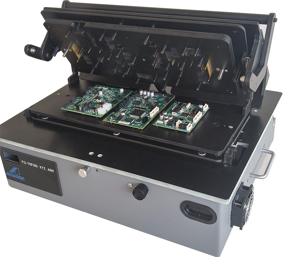
Your UUT is in safe hands, mechanically
The non-wiping mechanism involves a controlled, uniform, and consistent vertical movement during PCB testing. This ensures that all test points on the PCB are contacted simultaneously and with equal force by the test probes or pogo pins. This uniform contact is critical for the following reasons:
Consistent Test Results: By ensuring that each test point receives the same amount of pressure, the non-wiping mechanism contributes to the accuracy and repeatability of test results. This is crucial for identifying faults and verifying the functionality of the UUT.
Minimizing Wear and Tear: A key feature of the non-wiping action is that the test probes make contact with the test points without sliding across them. This reduces wear and tear on both the probes and the PCB, minimizing the risk of damage. As a result, the lifespan of the test fixture and the UUT is extended, reducing the frequency of replacements and repairs.
Enhanced Reliability: The linear collapse design, which incorporates the non-wiping mechanism, ensures precise alignment and reliable connections during testing. This mechanism maintains the integrity of the contact points, contributing to the overall reliability of the testing process.
Protection of Test Components: By avoiding lateral movement or sliding, the non-wiping mechanism protects sensitive components on the PCB. This is particularly important for high-density boards where test points are closely spaced, and any sliding action could cause shorts or other damage.
In summary, the non-wiping mechanism in UUT test fixture design is essential for maintaining the reliability, precision, and efficiency of the testing process. It ensures high-quality results while protecting both the test fixture and the unit under test, ultimately contributing to more robust and reliable electronic products. Whether using a bed of nails or flying probe testing, the principles of controlled, precise contact are critical for achieving accurate and repeatable test results.
Keypoints to note:
- Ensures all test points on the PCB are contacted simultaneously with equal force, providing reliable and repeatable test results.
- Probes make contact without sliding across test points, reducing wear and tear on both the probes and the PCB.
- Maintains precise alignment of test probes, minimizing the risk of damage and ensuring accurate testing.
- Extends the lifespan of the test fixture and the unit under test by minimizing mechanical stress and wear.
Design and manufacture of such non-wiping fixtures typically take four to six weeks.
Your UUT is in safe hands, mechanically
The non-wiping mechanism involves a controlled, uniform, and consistent vertical movement during PCB testing. This ensures that all test points on the PCB are contacted simultaneously and with equal force by the test probes or pogo pins. This uniform contact is critical for the following reasons:
Consistent Test Results: By ensuring that each test point receives the same amount of pressure, the non-wiping mechanism contributes to the accuracy and repeatability of test results. This is crucial for identifying faults and verifying the functionality of the UUT.
Minimizing Wear and Tear: A key feature of the non-wiping action is that the test probes make contact with the test points without sliding across them. This reduces wear and tear on both the probes and the PCB, minimizing the risk of damage. As a result, the lifespan of the test fixture and the UUT is extended, reducing the frequency of replacements and repairs.
Enhanced Reliability: The linear collapse design, which incorporates the non-wiping mechanism, ensures precise alignment and reliable connections during testing. This mechanism maintains the integrity of the contact points, contributing to the overall reliability of the testing process.
Protection of Test Components: By avoiding lateral movement or sliding, the non-wiping mechanism protects sensitive components on the PCB. This is particularly important for high-density boards where test points are closely spaced, and any sliding action could cause shorts or other damage.
In summary, the non-wiping mechanism in UUT test fixture design is essential for maintaining the reliability, precision, and efficiency of the testing process. It ensures high-quality results while protecting both the test fixture and the unit under test, ultimately contributing to more robust and reliable electronic products. Whether using a bed of nails or flying probe testing, the principles of controlled, precise contact are critical for achieving accurate and repeatable test results.
Let’s work together on your
next project
We have been providing our customers with test fixtures for over 20 years. We have a proven track record of providing excellent customer service, quality products, and reasonable prices.